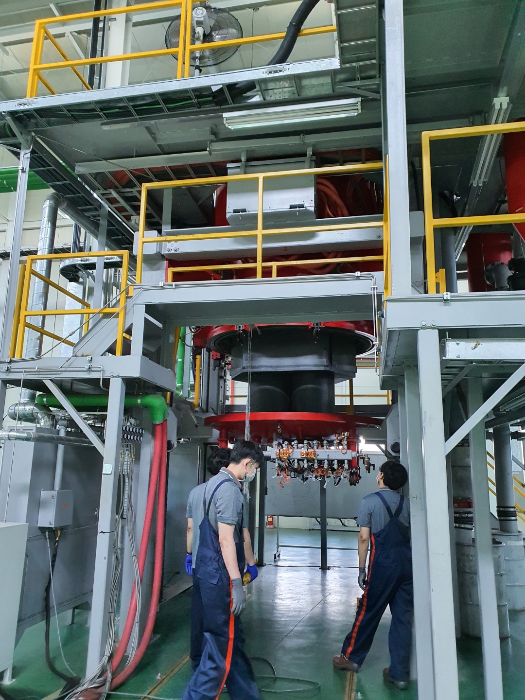
KM Innovation grows zinc selenide by chemical vapor deposition in South Korea. The plant is 20,000 m² (2023.06 introduction). H2Se is made on site. Florida quotes and ships. What follows is the published chemistry, the 1977 DTIC rates, and what the 2023.06 KM introduction actually says. Diagrams are illustrative. Plant photographs are real.
The reaction
Large IR ZnSe plates sold for CO2 optics are made by CVD, not by pouring a melt. ZnSe melts near 1525 °C; Published notes already put oxidation at 300 °C and dissociates around 700 °C in air. Bulk optics of this area are grown from vapor. The reaction Miles et al. wrote down in 1977 (DTIC ADA042147) is still the one in the patents:
Zn (g) + H2Se (g) → ZnSe (s) + H2 (g)
Zinc vapor is generated by heating the metal under reduced pressure and carrying it into the deposition zone. Hydrogen selenide meets it at a hot mandrel. Hydrogen and unused process gas are pumped away. The deposit is polycrystalline. Typical grain in the ADA042147 laser-quality table was ~70 µm; KM publishes < 100 µm. A later Ceramics 2022 review of laser-quality CVD (Gavrishchuk et al.) puts the useful window at about 650–750 °C, grain 30–50 µm on some Russian lots, and notes the process window for laser quality in a large reactor is narrow.
Published growth rates — CVD is not CVT
Laser-quality CVD is the slow end of the process. Faster deposition is how scatter and absorption rise. ADA042147: “For laser quality material the deposition process is carried out at 750 °C at a deposition rate of approximately 0.005 in/hr.” That is ~127 µm/h. The same table lists density 5.27 g/cm³, 10.6 µm absorption 4×10⁻⁴ cm−1, grain 70 µm, Knoop 100. RU2253705C1 specifies 50–70 µm/h for optical quality and records 26 mm grown at 55 µm/h. Chinese process patents CN114016129B and CN112795897A sit with that 50–200 µm/h band; above ~200 µm/h they say quality falls off. ADA083005’s “typical” 0.005–0.010 in/h (127–254 µm/h) and “inch-class in less than two weeks” is the fast production reading. We do not use 254 µm/h on the home clock. At 50 µm/h, 30 mm is 600 h of furnace-on (~25 days) if the rate holds the whole thickness. At the RU midpoint 60 µm/h, ~21 days. At ADA042147 laser-quality 127 µm/h, ~10 days. Heat-up, cool-down, grind and inspect are extra. That arithmetic is not a KM lead time.
People still quote “a year to grow 45 mm.” That number matches chemical vapor transport of single-crystal ZnSe, not bulk CVD. Fujiwara, Namikawa, Hirota, Irikura, Matsumoto and Kotani, J. Crystal Growth 196, 83–87 (1999), grew 1-inch ZnSe by iodine CVT with a self-moving convection shield. They state the slow rate — about 0.1 mm/day — was required for morphological stability. 45 mm at 0.1 mm/day is 450 days. Different chemistry, different product, different RFQ. We do not sell that crystal.
What the KM introduction actually says
The 2023.06 company introduction: CVD-ZnSe factory established in South Korea in 2012 (then PhoenixTek); export from 2017; ownership change 2018; high-thickness production recorded 2020; name KM INNOVATION from 2022. Feedstock Se 99.999% and H2 99.995%. KM states they are the only H2Se manufacturer in South Korea. CVD capacity up to 1,000 kg/month. Size up to Dia 800 × 30 mm T (the intro also notes max 45 mm T). Domes custom-made. After growth the machining factory lists water-jet cutting, centering, milling, and polishing up to Dia 300 mm. The KM datasheet lists grain < 100 µm, bulk absorption < 0.0005 cm−1 at 10.6 µm, n = 2.403 at 10.6 µm. Lot data is stated on the quotation. We do not put mandrel temperatures, H2Se generator rates or furnace-on hours on this page.
After the deposit
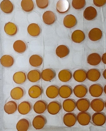
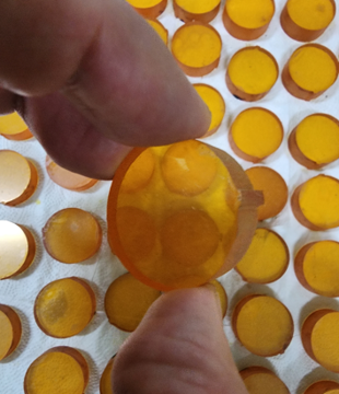
What you buy is polycrystalline CVD ZnSe. Laser grade vs optical grade is a selection on that material (absorption at 10.6 µm vs imaging use), not a second chemistry.
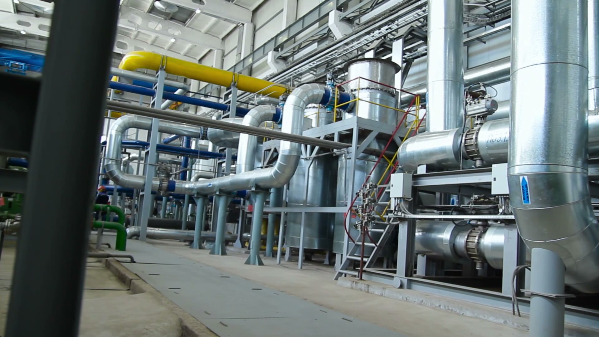
Photographs from the plant show the next steps we actually sell: water-jet nesting (SMTY, min. +1.5 mm oversize), core-drilled blanks, and finished windows. That is why CVD exists at this scale: area first, then nest.
Process schematic
Zn vapor + H2Se. KM feedstock on the 2023 intro: Se 99.999%, H2 99.995%.
Zn (g) + H2Se (g) → ZnSe (s) + H2 (g). The layer builds on a mandrel.
Polycrystalline plate. Datasheet max Dia 800 × 30 mm T. Then grind, water-jet, core.
Illustrative process boxes only — not KM furnace internals. Literature quality CVD is weeks of furnace-on time at 50–70 µm/h (RU2253705C1) or ~10 days at 127 µm/h (ADA042147 laser-quality), for 30 mm, if the rate holds. Heat-up, cool-down and grind are extra. A year-scale number matches published single-crystal CVT (~0.1 mm/day), a different process. Thickness clock · Factory photos
The reactor photograph is from the plant floor. Inventory photos and the “crystal push” plant film show the deposit after the run. Lot absorption and index come on the quotation against the KM datasheet.
References. Miles, P. et al., DTIC ADA042147 (1977) — 750 °C, ~0.005 in/h laser-quality CVD ZnSe, α ≈ 4×10⁻⁴ cm−1, grain ~70 µm. RU2253705C1 — 50–70 µm/h quality window; 26 mm at 55 µm/h. DTIC ADA083005 — 0.005–0.010 in/h production range (fast end not used as the quality default here). Fujiwara, S. et al., J. Crystal Growth 196, 83–87 (1999) — iodine CVT ~0.1 mm/day. CN114016129B; CN112795897A. Gavrishchuk et al., Ceramics 5, 35 (2022), 650–750 °C CVD window. KM Innovation introduction Rev. 2023.06 and ZnSe datasheet.