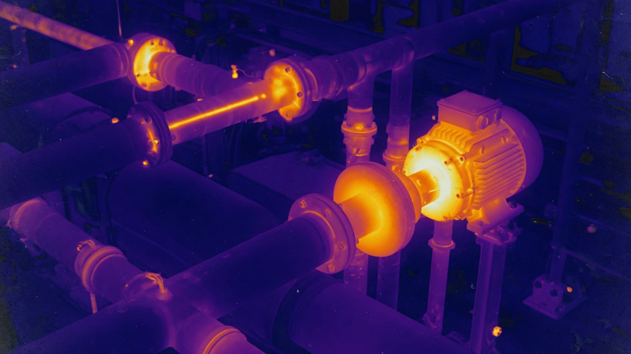
One transmission window, two jobs. 10.6 µm lasers punish absorption. 8–12 µm cameras punish scatter and the wrong AR. “IR” is not a wavelength.
CO2 at 10.6 µm
You need laser-grade absorption (< 5×10⁻⁴ cm−1 on the KM sheet; published tables ~5×10⁻⁴), a coating that actually hits 10.6 µm, and usually a visible HeNe path through the same optic. Thermal lensing is the design constraint once the AR is honest: dn/dT ≈ +61×10−6 K−1 at 10.6 µm, k = 20 W m−1 K−1 on the KM sheet (published tables often 18). Uncoated, n = 2.403 gives ~17% per face and ~(1−R)² ≈ 69% through two faces. Do not put an uncoated plate in a resonator and call it a test.
Thermal / LWIR, 8–12 µm
You need scatter control, cosmetic quality, and often a different AR. Optical grade is the default. Published short-wave absorption (5.0×10⁻³ cm−1 at 1.3 µm) does not matter in LWIR; grain scatter and index homogeneity do. A camera window that “worked on the FTIR” can still be a bad laser lens. The reverse is also true: a laser V-coat can starve a broadband imager. Dual-band 8–12 µm AR is not a 10.6 µm V-coat.
Why not Ge, ZnS, Si
| Material | Does well | Gives up |
|---|---|---|
| ZnSe | 0.6–16 µm, HeNe + CO2, low α at 10.6 | Soft (Knoop ~110), toxic, large dn/dT |
| Ge | n ≈ 4 in LWIR, Knoop ~780, cheap LWIR cameras | Opaque in the visible; thermal runaway |
| ZnS (CVD / MS) | Harder, some visible, rain/sand | Usually more scatter / absorption at 10.6 than laser ZnSe |
| Si | MWIR, cheap, hard | Cuts off before LWIR / 10.6 |
Germanium is the usual LWIR competitor. Index is about 4.00 at 10 µm, 4.03 at 4 µm. Knoop ~780. It is opaque below ~2 µm, so there is no HeNe through the same window. The failure mode that ends the CO2 argument is thermal runaway. P. A. Young, Appl. Opt. 10, 638–643 (1971), measured 50 Ω·cm Ge from 300–450 K and showed that at 10.6 µm the absorption is free-carrier, not lattice. For each cooling scheme there was a critical power density Pc; above it the window ran away. Highest Pc in that paper was 88 W/cm² with the germanium cooled below ambient. Handbook language since then is that Ge transmission starts to sag near 70–100 °C and falls apart by 200–300 °C (Photonics Handbook IR-materials review; Harris, SPIE). ZnSe does not have that free-carrier cliff at 10.6 µm. That is why high-power CO2 still buys ZnSe.
CVD ZnS is harder and better in rain. It was industrialized in parallel with ZnSe (Harris, ch. 6). It is usually the wrong buy for a kW-class 10.6 µm lens. Silicon is an MWIR crystal. We quote ZnSe. Wavelength on the print: 10.6 µm or 8–12 µm, not “IR.”
References. Young, P.A., “Thermal Runaway in Germanium Laser Windows,” Appl. Opt. 10, 638–643 (1971). Harris, D.C., Materials for Infrared Windows and Domes, SPIE (1999). KM Innovation ZnSe datasheet.